CN
-
Service Hotline
15766086363

Release Date:Sep 19, 2025
PCB copying, also commonly referred to as circuit board copying, circuit board cloning, circuit board duplication in the industry PCB cloning, PCB reverse design, or PCB reverse research and development. There are various definitions of PCB copying in the industry and academia, but none of them are complete. To give an accurate definition of PCB copying, one can refer to the authoritative PCB copying laboratory in China: PCB copying refers to the use of reverse research and development technology to reverse analyze the circuit board on the premise that there are already physical electronic products and circuit boards. The original product's PCB files, bill of materials (BOM) files, schematic files, and PCB silk screen production files are restored 1:1, and then these technical files and production files are used for PCB making, component soldering, flying pin testing, circuit board debugging, and to complete the original circuit board sample. Complete replication. Due to the fact that electronic products are composed of various circuit boards that form the core control part for operation, the process of PCB copying can be used to extract the complete set of technical information for any electronic product, as well as to replicate and clone the product.
PCB copying is a reverse research technique that uses a series of reverse research techniques to obtain the PCB design circuit, circuit schematic, and BOM table of an excellent electronic product. Through this reverse research method, a product that others need two or three years to develop can be learned in just one month through PCB copying reverse research. This has played a very important role in promoting developing countries to catch up with the world. Moreover, the development of reverse research technology has also played a promoting role in the technological breakthroughs of those development teams. The vigorous development of reverse research technology has also led to the continuous updating of forward research technology. The competitive relationship between forward research and reverse research has enabled the rapid development of electronic technology in recent years. Electronic products are updated almost once a year, and the speed of electronic product updates will only become faster in the future. Because PCB copying lowers the threshold of electronic technology. PCB copying has enabled more and more developing countries to quickly step onto the forefront of high-tech electronic technology and work together with developed countries to research electronic technology. The larger the research team, the more advanced the electronic technology in this world can be.
For PCB copying, many people do not understand what PCB copying is, and some even believe that PCB copying is a knockoff. In people's understanding, 'shanzhai' means imitation, but PCB copying is definitely not imitation. The purpose of PCB copying is to learn the latest electronic circuit design technology from abroad, absorb excellent design solutions, and then use them to develop and design better products.
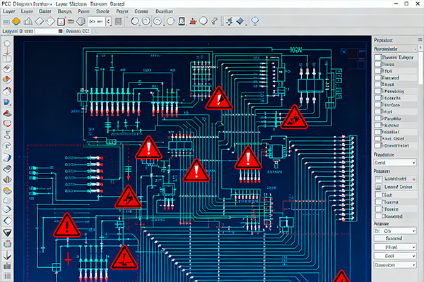
The technical implementation process of PCB copying board
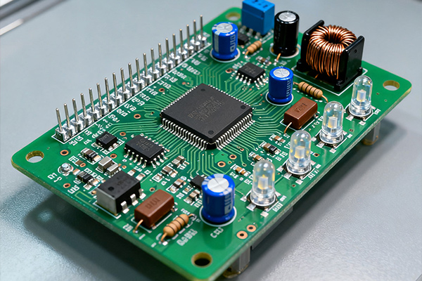
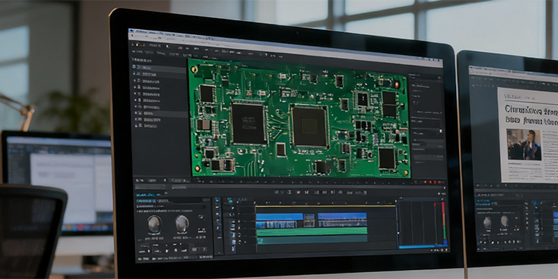
Simply put, it means scanning the circuit board to be copied first, recording the detailed positions of the components, then disassembling the components to make a bill of materials (BOM) and arranging material procurement. The empty board is scanned into a picture and processed by the copying software to restore it to a PCB board diagram file. Then, the PCB file is sent to the plate making factory to make the board. After the board is made, the purchased components are soldered onto the finished PCB board, and then tested and debugged on the circuit board.
The specific technical steps are as follows:
The first step is to obtain a PCB and record the model, parameters, and position of all components on paper, especially the direction of diodes, transistors, and IC notches. It is best to take two photos of the positions of the components with a digital camera. Many PCB circuit boards are getting more advanced, and some of the diodes and transistors on them cannot be seen without paying attention.
Step two, dismantle all components and remove the tin from the PAD holes. Clean the PCB with alcohol and place it in the scanner. When scanning, slightly increase the scanning pixels to obtain clearer images. Gently polish the top and bottom layers with water gauze until the copper film is shiny, then place them in the scanner, start PHOTOSHOP, and scan the two layers separately in color. Note that the PCB must be placed horizontally and vertically inside the scanner, otherwise the scanned image cannot be used.
Step three, adjust the contrast and brightness of the canvas to create a strong contrast between the areas with and without copper film. Then, convert the secondary image to black and white and check if the lines are clear. If not, repeat this step. If the image is clear, save it as a black and white BMP format file TOP BMP and BOT BMP. If you find any problems with the image, you can use PHOTOSHOP to repair and correct them.
Step 4, convert the two BMP files into PROTEL files, and call in two layers in PROTEL. If the positions of PAD and VIA passing through the two layers basically coincide, it indicates that the previous steps are well done. If there is any deviation, repeat the third step. So PCB copying is a very patient job, because even a small problem can affect the quality and matching degree after copying.
Step 5, convert the BMP of the TOP layer to the TOP PCB, paying attention to converting it to the SILK layer, which is the yellow layer. Then, draw lines on the TOP layer and place the devices according to the drawing in step 2. After drawing, delete the SILK layer. Repeat until all layers are drawn.
Step six, transfer the TOP PCB and BOT PCB into PROTEL and merge them into one image.
Step seven, use a laser printer to print the TOP LAYER and BOTTOM LAYER onto transparent film (1:1 ratio), place the film on that PCB, and compare if there are any errors. If they are correct, you have completed the task.
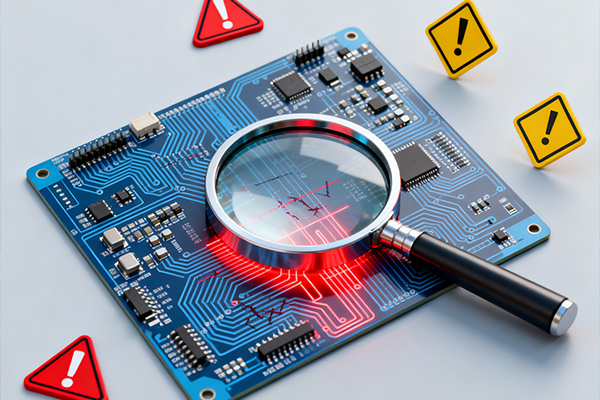
A copied board identical to the original board was born, but this is only half completed. Further testing is required to ensure that the electronic technology performance of the copied board is the same as that of the original board. If it's the same, then it's really done.
Email: 1330695973@qq.com
Factory: Room 703, Kelunte R&D Building, No. 1 Ganli 5th Road, Jihua Street, Longgang District, Shenzhen City