CN
-
Service Hotline
15766086363

Release Date:Sep 19, 2025
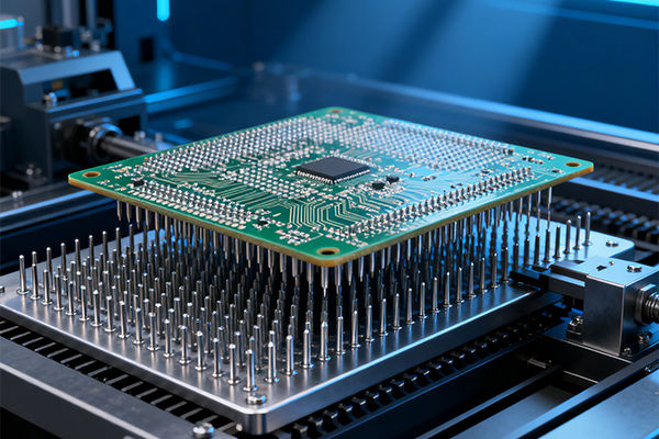
In PCB copying design, wiring is an important step in completing product design. It can be said that all the preparatory work is done for it. In the entire PCB, the wiring design process has the highest limit, the finest skills, and the largest workload. PCB wiring includes single-sided wiring, double-sided wiring, and multi-layer wiring.
There are also two ways of wiring: automatic wiring and interactive wiring. Before automatic wiring, wires with strict requirements can be pre wired interactively. The edges of the input and output terminals should avoid adjacent parallelism to avoid reflection interference.
If necessary, grounding should be added for isolation. The wiring between adjacent layers should be perpendicular to each other, and parallelism can easily cause parasitic coupling.
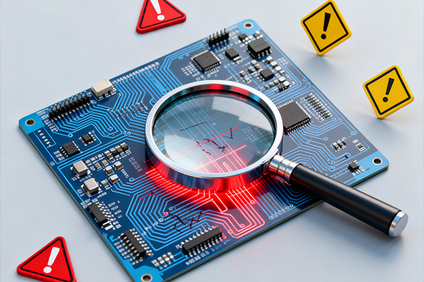
1. Common errors in PCB schematics:
(1) ERC report pin not connected to signal:
a. I/O properties were defined for the pins when creating the encapsulation;
b. Inconsistent grid properties were modified when creating or placing components, and the pins and wires were not connected;
c. When creating a component, the pin direction must be reversed and a non pin name terminal must be connected.
(2) Component running outside the drawing boundary: No component was created in the center of the component library chart paper.
(3) The created engineering file netlist can only be partially loaded into PCB: global was not selected when generating netlist.
(4) When using components composed of multiple parts created by oneself, do not use annotates
2. Common errors in PCB:
(1) When loading the network, report that the Node was not found:
a. The components in the schematic use packaging that is not available in the PCB library;
b. The components in the schematic use packaging with inconsistent names in the PCB library;
c. The components in the schematic use packaging with inconsistent pin numbers in the PCB library. For example, in a transistor, the pinnumbers in SCH are e, b, and c, while in PCB they are 1, 2, and 3.
(2) Always unable to print on a single page of paper during printing:
a. When creating the PCB library, it was not at the origin point;
b. The components have been moved and rotated multiple times, and there are hidden characters outside the PCB board boundary. Select to display all hidden characters, shrink the PCB, and then move the characters within the boundaries.
Email: 1330695973@qq.com
Factory: Room 703, Kelunte R&D Building, No. 1 Ganli 5th Road, Jihua Street, Longgang District, Shenzhen City