CN
-
Service Hotline
15766086363


Release Date:May 26, 2026
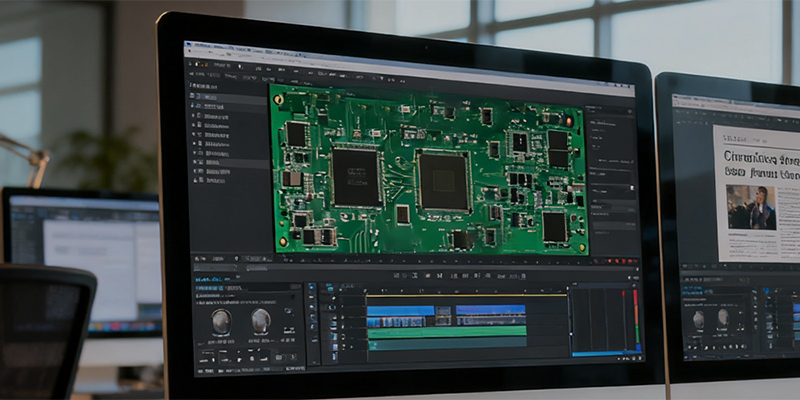
Flying probe test verification is a crucial link in the PCB cloning process, serving as the final quality check to ensure that the cloned PCB is functionally consistent with the original board. Unlike traditional bed-of-nails testing, flying probe testing uses movable probes to conduct electrical tests on the PCB without the need for custom test fixtures, making it flexible and suitable for small-batch and prototype testing, especially for complex and high-density PCBs.
The flying probe test verification process starts with the preparation of test data. Engineers import the cloned PCB’s Gerber files and netlist into the flying probe test system, which automatically generates a test program based on the circuit connections. The system then uses high-precision movable probes to contact the test points, pads, and pins on the PCB, conducting continuity tests, insulation tests, and short-circuit tests to verify the correctness of the circuit connections. For cloned PCBs with complex structures such as blind and buried vias, the test system uses multi-probe synchronization technology to ensure that all layers of connections are fully tested.
During the test, the system records all test data and generates a detailed test report, marking any abnormal points such as open circuits, short circuits, or poor contact. Engineers then analyze the test results, identify the causes of abnormalities, and modify the cloned PCB design accordingly. This iterative process ensures that the final cloned PCB has no electrical defects. In addition, flying probe testing can also verify the soldering quality of components, ensuring that the assembled PCB meets the functional requirements of the original board. This verification method not only improves the accuracy and reliability of PCB cloning but also shortens the development cycle by reducing the need for custom test fixtures.

Email: 15361682656@163.com
Factory: Room 703, Kelunte R&D Building, No. 1 Ganli 5th Road, Jihua Street, Longgang District, Shenzhen City