CN
-
Service Hotline
15766086363

Release Date:May 25, 2026
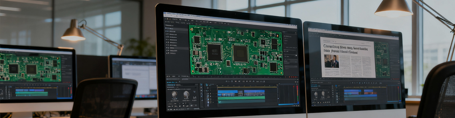
High-frequency PCB reverse cloning is a specialized technology aimed at replicating circuit boards used in high-frequency signal transmission scenarios, typically with operating frequencies above 1GHz, such as communication equipment, radar systems, and microwave devices. The core challenge of high-frequency PCB cloning lies in maintaining signal integrity, minimizing signal loss, crosstalk, and electromagnetic interference (EMI), which requires in-depth understanding of high-frequency circuit principles and strict control over the cloning process.
The reverse cloning process begins with the analysis of the original high-frequency PCB’s material properties and structural characteristics. Engineers first identify the substrate material (such as Rogers or FR-4 with high dielectric constant stability) and record key parameters such as dielectric constant, loss tangent, and thickness, as these factors directly affect signal transmission efficiency. They then use high-precision measurement tools to map the trace width, spacing, and impedance matching of the original board, which are critical for ensuring high-frequency signal quality.
In the schematic reconstruction and layout cloning stage, engineers use professional EDA software to replicate the circuit connections, focusing on optimizing the signal path length to reduce transmission delay and signal distortion. They also pay special attention to the grounding design and shielding structure of the original board to minimize EMI. After the layout is completed, simulation analysis is conducted to test signal integrity, including impedance matching, crosstalk, and insertion loss. Finally, prototype production and high-frequency performance testing are carried out using specialized equipment to ensure that the cloned PCB meets the same frequency response and signal transmission performance as the original, supporting the stable operation of high-frequency electronic systems.

Email: 15361682656@163.com
Factory: Room 703, Kelunte R&D Building, No. 1 Ganli 5th Road, Jihua Street, Longgang District, Shenzhen City