CN
-
Service Hotline
15766086363

Release Date:May 26, 2026
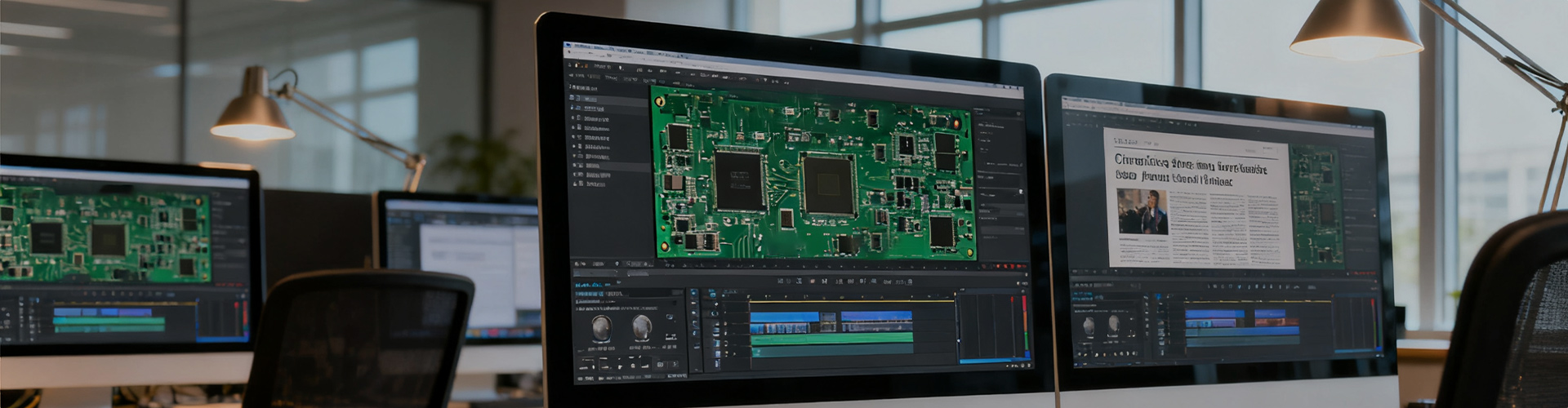
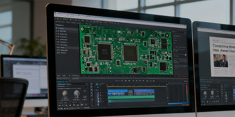
PCB file export is a key step in the circuit board cloning process, referring to the process of generating standard design files from the reversed PCB layout, which can be directly used for PCB manufacturing and assembly. The exported files include Gerber files, drill files, BOM (Bill of Materials) lists, and schematic diagrams, which are essential for ensuring the consistency between the cloned PCB and the original board in terms of structure and function.
Before exporting the PCB files, engineers need to complete the layout reconstruction and verification of the cloned PCB. They use EDA software to carefully check the circuit connections, component footprints, trace widths, and spacing to ensure that all parameters are consistent with the original board. Special attention is paid to the layer settings, via parameters, and silk screen information to avoid errors during the manufacturing process. For multi-layer PCBs, engineers also need to confirm the layer stack-up order and interlayer connections to ensure the correctness of the exported files.
The export process follows industry standards to ensure compatibility with PCB manufacturing equipment. Gerber files, which include data for each copper layer, silk screen layer, solder mask layer, and solder paste layer, are exported in standard formats (such as RS-274X) to ensure that the manufacturer can accurately interpret the design information. Drill files (in .drl format) are exported to specify the position, size, and type of each hole. BOM lists are generated to record the model, parameters, and quantity of each component, facilitating component procurement and assembly. Finally, the exported files are reviewed and verified to ensure that there are no missing or incorrect data, laying a solid foundation for the mass production of the cloned PCB.

Email: 15361682656@163.com
Factory: Room 703, Kelunte R&D Building, No. 1 Ganli 5th Road, Jihua Street, Longgang District, Shenzhen City