CN
-
Service Hotline
15766086363

Release Date:Sep 19, 2025
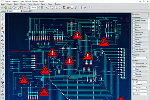
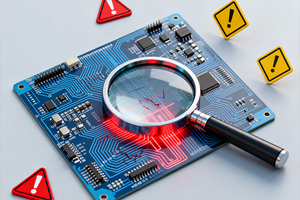
Faced with high-density PCBs, needle bed testing technology is constantly developing and improving, mainly reflected in the increase of needle bed density, innovation and optimization of fixture design and manufacturing technology, introduction of auxiliary testing, adoption of data optimization technology, and improvement of testing technology (switch card) technology.
(1) The needle bed density has increased.
The center distance of a typical needle bed probe is 2540ym, known as a single density needle bed. With the increase of test points and the improvement of test density, many manufacturers have launched dual density needle beds with a center to center distance of 17781im for probes. Now, some manufacturers are also developing four density testing equipment, which can solve the problem of test points to some extent, but the issue of accuracy still exists.
(2) Innovation in fixture design and manufacturing technology.
As the main influencing factor of testing accuracy, the design and manufacturing of fixtures are extremely critical. In many needle bed testing equipment that have successfully undergone high-density testing, the fixture design often has unique features. For example, ECT's fixture design software carefully considers issues such as the inclination and friction of the test probe, ensuring that the center of the produced fixture and probe are aligned with the test point, ensuring accuracy and consistency with the design. In areas with fewer probes, the fixture is subjected to balanced forces in the X, Y, and Z directions, without bending deformation and deviation. The automatic alignment system can also detect and compensate for deviations between the positioning hole and the outer graphic. In the selection of fixture materials, modular materials that are less affected by temperature and humidity are used to ensure accurate and stable dimensions.
(3) Introduction of conductive rubber module.
In some needle bed testing equipment, for extremely fine parts such as TAB, flip chip, yBGA, or QFP, the center distance of the testing points is around 0.1mm, making it difficult to locate with probes for testing. The use of conductive rubber modules for local testing can overcome the shortcomings of needle bed testing. This module is connected to the fixture through a pneumatic conduit and automatically controlled for positioning by the corresponding fixture design software. If multiple areas require the use of this module, it can be used multiple times. But the conductive rubber module short circuits all the test points in the covered area, and the short circuit inside the tested device cannot be detected. It is only used to test the connectivity between the tested area and the outside world. To test the internal short circuit, these nets must be selected and other methods (such as moving probes) must be used for testing.
(4) Improvement of switch card technology.
To meet the requirements of testing accuracy, the switch card is required to be able to withstand high voltage, have no leakage in the "off" state, and compensate for the resistance in the "on" state to ensure accurate testing. The switch card itself is packaged in SMT, occupies a small volume, and has ESD (electrostatic discharge protection).
Due to the limitations of its principles and methods, needle bed testing technology faces severe technical challenges, but certain aspects (such as efficiency) still have advantages that other methods do not have. In addition, with the improvement of fixture technology and the combination of new technologies, it still has strong vitality in the testing field.
Email: 1330695973@qq.com
Factory: Room 703, Kelunte R&D Building, No. 1 Ganli 5th Road, Jihua Street, Longgang District, Shenzhen City