CN
-
Service Hotline
15766086363

Release Date:Aug 17, 2026
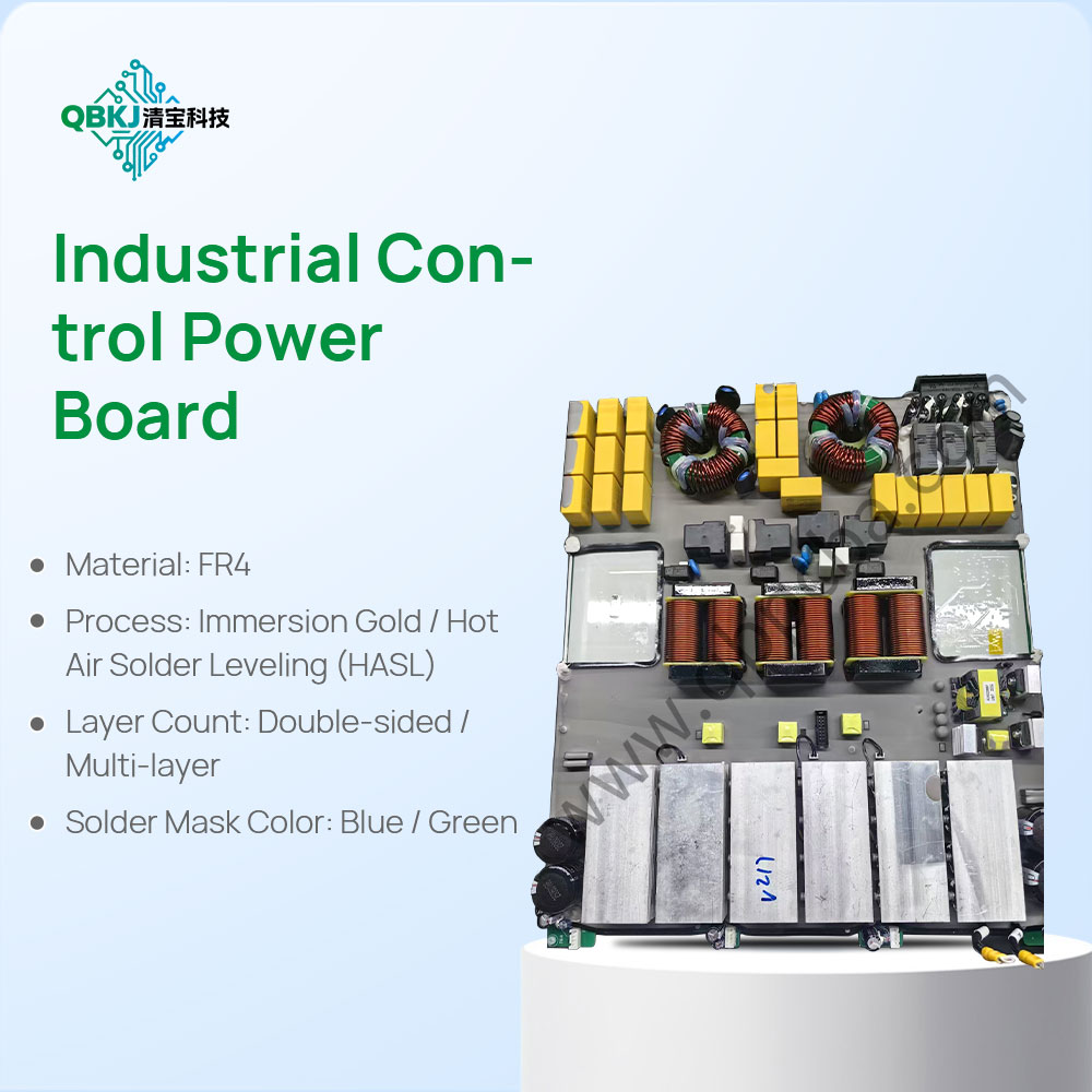
Thick copper substrate PCB clone is a professional reverse engineering technology for high-current, high-power thick copper circuit boards, which is widely used in power supply equipment, inverter equipment, new energy vehicles, industrial motor control, and high-current power module fields. Ordinary PCB boards usually use 1oz-2oz copper foil, while thick copper substrate PCBs adopt copper foil with a thickness of 3oz-10oz or even thicker. They have ultra-high current carrying capacity, excellent heat dissipation performance, and strong overload resistance, and can work stably in high-current and high-temperature heat-generating environments. The cloning technology of thick copper substrates is greatly different from conventional PCB cloning, which needs to solve the technical problems of thick copper circuit etching, layer alignment, lamination stability, and current carrying performance restoration.
The core difficulty of thick copper substrate PCB clone lies in the accurate restoration of thick copper circuit structure and electrical performance. In the preliminary analysis stage, it is necessary to accurately detect the copper foil thickness of each circuit layer of the original thick copper board, the thickness of the dielectric substrate, the size of the large current-carrying copper foil area, and the parameters of heat dissipation copper blocks. The current carrying capacity of thick copper circuits is directly determined by the copper foil thickness and circuit width. Slight errors in copper thickness and line size will lead to insufficient current carrying capacity of the cloned board, resulting in heating burnout and equipment failure in the working process. Therefore, high-precision thickness gauges and microscopic measuring instruments are used to calibrate all thick copper circuit parameters one by one in the early stage of cloning.
In the layer stripping and data acquisition stage of thick copper substrates, mechanical and chemical composite non-destructive stripping technology is adopted. Due to the thick copper layer and strong rigidity of the thick copper board, the traditional single chemical stripping method is slow and easy to cause copper layer corrosion, while mechanical stripping is easy to damage the substrate and fine lines. The composite stripping technology can effectively separate the thick copper circuit layer and the dielectric layer, ensure the integrity of the thick copper circuit and tiny auxiliary lines, and provide complete and accurate original data for subsequent reverse modeling. After stripping, full-layer scanning and data modeling are carried out to record the layout of high-current main circuits, auxiliary control circuits, heat dissipation areas, and via hole conduction structures in detail.
The production process of thick copper substrate cloned boards is the key to ensure product quality. The etching process of thick copper circuits is the most difficult link. Ordinary etching processes are prone to incomplete etching, line side corrosion, and uneven line width for thick copper layers. Therefore, a multi-stage differential etching process is adopted. The etching speed and solution concentration are adjusted in stages according to the copper thickness to ensure that the thick copper main circuit has neat edges, consistent width, and no residual copper and side corrosion. At the same time, for the large-area copper-clad heat dissipation area, the etching uniformity is strictly controlled to avoid local thin copper affecting heat dissipation and current conduction.
The lamination process of thick copper substrates also has special process standards. The thick copper layer has large stress, which is easy to cause board warping, interlayer dislocation, and delamination during lamination. In the cloning production, low-stress lamination materials are selected, and segmented temperature rise and constant pressure lamination technology are adopted. The lamination pressure and time are adjusted according to the copper thickness and board size to fully release the internal stress of the thick copper layer, ensure the tight bonding between layers, and avoid board deformation and interlayer separation after production. In the drilling and via hole metallization process, high-precision drilling and thick copper electroplating technology are used to ensure that the via hole copper layer is thick and uniform, with strong conductivity, to meet the high-current conduction requirements.
After the completion of thick copper substrate cloning, strict electrical performance and reliability tests are required, including high-current load test, long-term heating test, insulation resistance test, and board flatness test. The high-current load test verifies that the cloned board can bear the rated current of the original board without overheating and voltage drop. The long-term aging test ensures the stable operation of the thick copper circuit under high-load working conditions. Thick copper substrate PCB clone focuses on the restoration of current carrying capacity and heat dissipation performance, which realizes the accurate replication of high-power circuit boards and meets the batch production and equipment maintenance needs of new energy and industrial power equipment.

Email: 15361682656@163.com
Factory: Room 703, Kelunte R&D Building, No. 1 Ganli 5th Road, Jihua Street, Longgang District, Shenzhen City