CN
-
Service Hotline
15766086363

Release Date:Jun 25, 2026
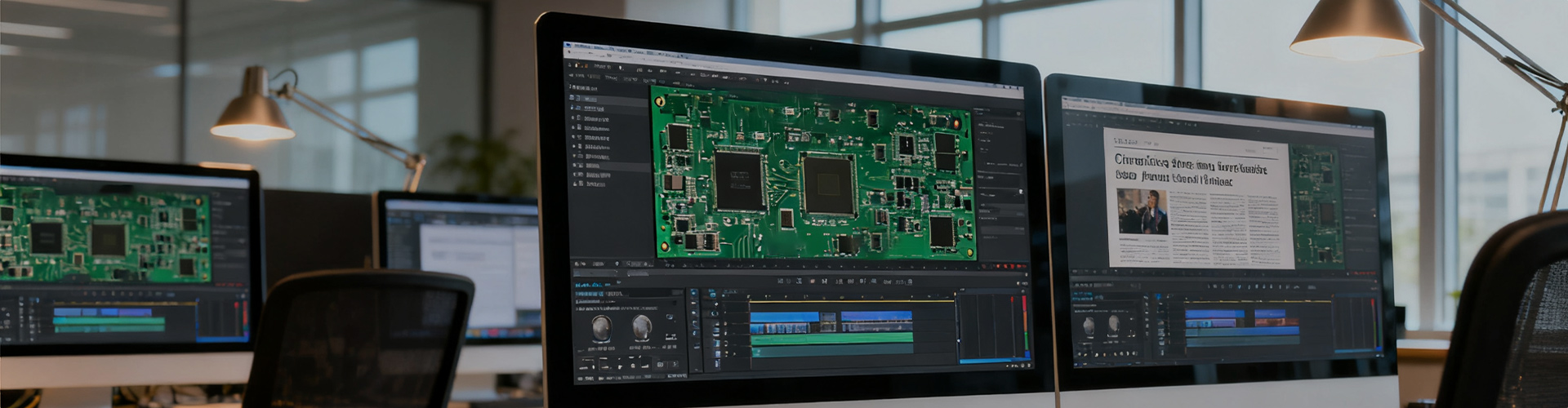
Precise scanning and replication of PCB copper foil circuits is the basic core technology of high-precision PCB cloning, which determines the circuit accuracy, electrical performance and operational stability of the final cloned board. Copper foil circuit is the core conductive carrier of PCB, including signal lines, power lines, grounding copper foil and isolation copper foil. The thickness, width, path, spacing and integrity of copper foil circuits directly affect the board’s current carrying capacity, signal transmission efficiency, anti-interference performance and heat dissipation effect. Traditional manual copying and ordinary scanning are prone to errors such as line width deviation, copper foil missing, spacing inconsistency and circuit distortion, resulting in short circuit, open circuit, insufficient current carrying and signal instability of the cloned board. Our professional copper foil circuit precise scanning technology realizes micron-level full-detail restoration of original copper foil circuits.
The copper foil circuit precise scanning process adopts high-resolution industrial professional scanning equipment and intelligent circuit identification system to carry out omnidirectional non-destructive scanning of the original PCB. First, the original board is professionally cleaned to remove surface dust, oil stains, oxide layers and residual solder, ensuring that the copper foil circuit is completely exposed without shielding interference. Then, high-precision ultra-micro scanning is carried out on the board surface and inner layer copper foil circuits, with the scanning resolution up to micron level, which can accurately capture tiny copper foil lines, narrow-gap isolation zones, irregular copper laying areas and ultra-fine signal lines that cannot be identified by ordinary scanners. The system automatically records all copper foil circuit data including line width, line thickness, line length, spacing distance and copper foil coverage area.
After scanning and data collection, the professional engineering team conducts manual secondary calibration and intelligent data optimization on all copper foil circuit data. For special copper foil designs such as irregular arc lines, differential signal copper foil, high-current thick copper foil and hollow grounding copper foil, one-to-one manual inspection and correction are carried out to eliminate scanning errors and data distortion. At the same time, combined with electrical performance principles, we verify the rationality of copper foil circuit layout, ensure that the scanned and restored copper foil circuit completely conforms to the original board’s circuit logic and electrical design standards, and avoid hidden dangers such as insufficient current carrying and poor signal anti-interference caused by inaccurate copper foil restoration.
In the board manufacturing stage, we strictly follow the scanned copper foil circuit data for production, adopt high-precision etching and copper laying processes to ensure that the copper foil thickness, line accuracy and overall layout of the new board are completely consistent with the original board. After production, we use professional precision testing equipment to detect the copper foil line width tolerance, copper thickness uniformity, circuit continuity and spacing safety of the new board. All indicators meet or exceed the original board’s design standards. This precise scanning and replication technology effectively guarantees the electrical performance consistency of the cloned PCB, improves the yield and stability of replicated boards, and provides a solid technical foundation for high-quality full-board cloning of various complex PCBs.

Email: 15361682656@163.com
Factory: Room 703, Kelunte R&D Building, No. 1 Ganli 5th Road, Jihua Street, Longgang District, Shenzhen City