CN
-
Service Hotline
15766086363

Release Date:Jun 25, 2026
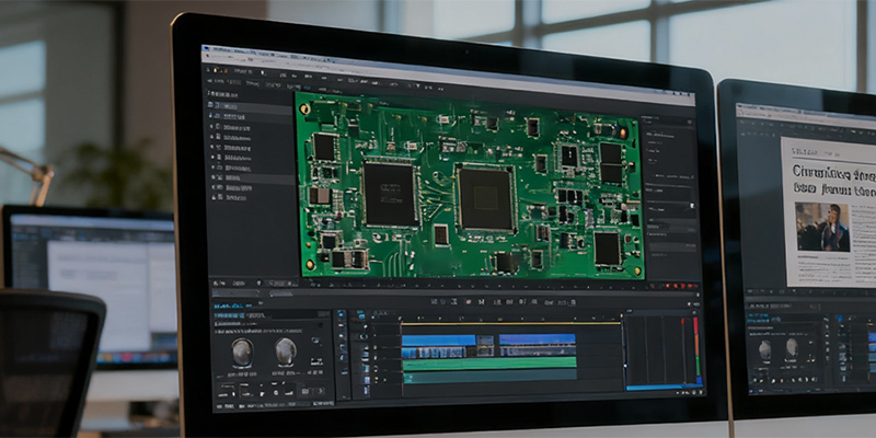
Multi-layer PCB inner layer circuit replication is a key high-precision service in PCB reverse engineering, aiming at the precise copying of 4-layer, 6-layer, 8-layer and even more high-layer complex circuit boards. Modern high-precision electronic equipment such as communication equipment, automotive electronics, industrial control main boards, and aerospace instruments mostly adopt multi-layer PCB designs. The inner layers bear core circuit connections such as power supply transmission, signal transmission, and grounding design. Different from single and double-layer PCBs with simple exposed circuits, multi-layer PCB inner layer lines are hidden inside the board body, with dense wiring, tiny line width, complex overlapping circuits and high precision requirements, which are difficult to detect and copy by ordinary scanning and copying technologies. Our professional multi-layer inner layer replication technology realizes non-destructive, high-precision and full-detail restoration of inner layer circuits, ensuring 100% consistency between replicated boards and original inner layer circuit logic.
The multi-layer inner layer replication process adopts a standardized layered detection and precise restoration process to ensure no missing or wrong lines in the inner layer. First, we carry out professional pretreatment on the original multi-layer board, including surface cleaning, solder mask removal, and component disassembly, to ensure that the board body is intact and the inner layer structure is not damaged. Then, through high-precision industrial X-ray scanning, microscopic layer-by-layer detection and professional circuit mapping technology, we conduct comprehensive scanning and data collection on each inner layer circuit. The system accurately identifies tiny lines, hidden vias, buried holes, blind holes, copper laying areas, isolation gaps and grounding circuits inside each layer, records the line width, line spacing, hole position coordinates and circuit connection relations of all inner layer circuits in real time, and eliminates detection dead angles and data errors caused by overlapping inner layers and shielding structures.
After completing the collection of all inner layer data, professional PCB engineers sort out and verify the layered circuit data one by one, build a complete multi-layer board hierarchical layout model, and calibrate the alignment accuracy between layers. The interlayer alignment precision is controlled within micron level to avoid functional faults such as signal short circuit, open circuit and crosstalk caused by interlayer deviation. For complex designs such as inner layer impedance lines, differential signal lines and high-current power lines, we conduct secondary parameter verification to ensure that the line thickness, copper thickness and wiring path completely match the original board’s electrical performance requirements. After the data verification is completed, standard multi-layer board production files are generated to guide the formal production of new boards.
In the manufacturing stage of multi-layer boards, we strictly follow the inner layer layout standards for layered pressing and processing, adopt high-precision lamination technology to ensure accurate alignment of each inner layer, and strictly control the pressing temperature, pressure and time parameters to avoid inner layer circuit deformation and offset. After the board is completed, we conduct layer-by-layer circuit detection, impedance testing, signal continuity testing and interlayer insulation testing on the new board to confirm that all inner layer circuits are completely consistent with the original board. This service is suitable for all types of high-precision multi-layer complex PCBs, solving the technical problems of inaccurate inner layer copying, missing lines and inconsistent interlayer performance in traditional copying, and providing reliable technical support for the replication and mass production of high-end multi-layer circuit boards.

Email: 15361682656@163.com
Factory: Room 703, Kelunte R&D Building, No. 1 Ganli 5th Road, Jihua Street, Longgang District, Shenzhen City