CN
-
Service Hotline
15766086363

Release Date:Aug 18, 2026
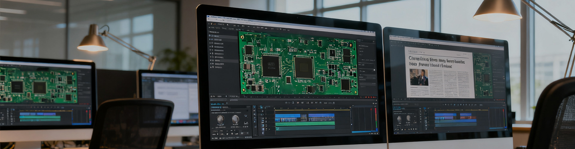
PCB copy board export CAD file is an important data output module in PCB reverse engineering (copy board) technology, which realizes the precise restoration and export of PCB structural layout, circuit wiring, pad distribution and mechanical size data into standard CAD editable files through reverse scanning, data measurement and circuit restoration of the original PCB sample. CAD file is the most universal and compatible engineering drawing file in the electronic manufacturing and mechanical processing industry, with powerful editable, modifiable and secondary development characteristics. The CAD file exported by PCB copy board can perfectly restore all physical and electrical layout characteristics of the original circuit board, providing basic data support for PCB secondary design, structural matching, process modification and engineering archiving.
The technical process of exporting CAD files from PCB copy board is rigorous and standardized, covering multiple links of physical measurement, data modeling and format conversion. First, professional equipment is used to perform full-scan measurement on the original PCB sample, including overall board size, board thickness, outline shape, special-shaped edge structure, positioning hole size and position, mounting hole distribution, slot and gap structure, and the three-dimensional spatial size of the PCB. At the same time, through circuit reverse analysis technology, the system accurately identifies the wiring trajectory, line width, line spacing, pad size, via hole parameters, solder mask opening range and silk screen printing content of each layer of the PCB, and establishes a complete digital model consistent with the physical board.
In the process of CAD file modeling and generation, technicians strictly follow international electronic engineering CAD drawing standards, classify and layer all PCB elements uniformly. The file is divided into independent layers such as outline layer, wiring layer (top and bottom signal layers, multi-layer inner layers), pad layer, via layer, solder mask layer, silk screen layer, mechanical processing layer and forbidden wiring layer, ensuring that each layer of data is independent, clear and editable. For special PCBs such as special-shaped PCBs, flexible PCBs, rigid-flex combined PCBs and multi-layer high-density PCBs, the CAD file will accurately restore complex structural features such as curved edges, folded structures, embedded holes and blind buried holes, and calibrate the dimensional tolerance of mechanical structures to ensure that the error between the digital model and the physical sample is controlled within the industrial precision range.
The exported PCB copy board CAD files support multiple mainstream CAD formats, including DWG, DXF and other universal formats, which are compatible with AutoCAD, Altium Designer, Cadence, KiCad and other mainstream electronic design and mechanical design software. Engineers can directly open, edit and modify the files, including adjusting wiring layout, optimizing component packaging, modifying board size, adjusting solder mask and silk screen content, and completing secondary design and performance optimization of the PCB. Different from the picture format and static drawing format, the CAD file exported by copy board has complete vector data characteristics, which can realize arbitrary scaling without distortion, precise dimensional measurement and parameter modification, and meet the needs of precision processing and design optimization.
In industrial practical application, PCB copy board export CAD file technology solves the technical dilemma of missing design documents of legacy PCBs and imported equipment PCBs. Enterprises can obtain complete editable design data of the original board through reverse derivation, which is convenient for product upgrading, function modification and structural optimization on the basis of the original mature circuit scheme. At the same time, CAD files can be seamlessly connected with subsequent mechanical structural design, fixture design and production processing, realizing the integrated design of PCB circuit and equipment structure, and greatly improving the overall R&D and production efficiency of electronic products. It is a core data carrier for realizing PCB reverse replication, secondary development and long-term technical archiving.

Email: 15361682656@163.com
Factory: Room 703, Kelunte R&D Building, No. 1 Ganli 5th Road, Jihua Street, Longgang District, Shenzhen City