CN
-
Service Hotline
15766086363

Release Date:Jun 10, 2026
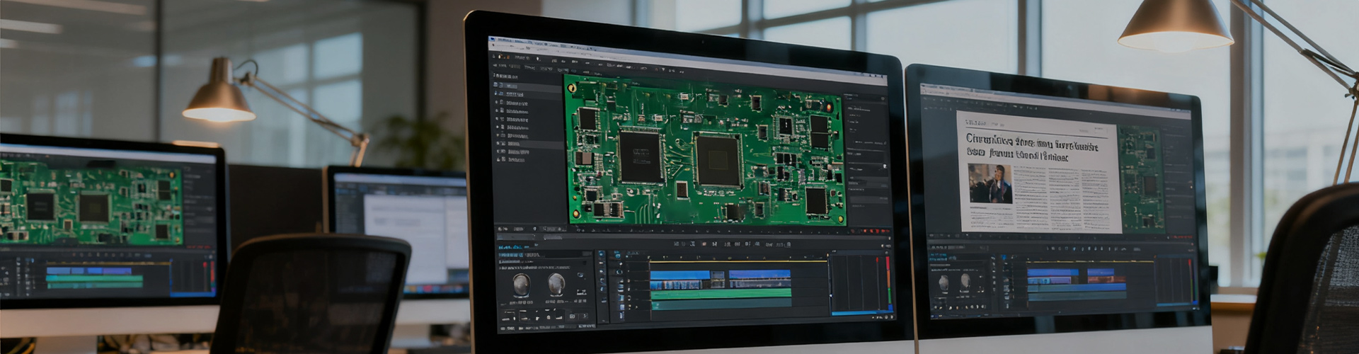
PCB copy paired with schematic drawing is a core precision engineering service that bridges physical circuit board entities and digital design documents, serving as the foundation of electronic product reverse engineering and secondary development. This service focuses on accurately extracting the complete circuit connection logic from finished or bare printed circuit boards, and converting discrete physical wiring into standardized, editable, and industrial-grade schematic diagrams. Unlike simple board copying that only replicates surface layouts, the matching schematic drawing work emphasizes the internal electrical correlation of components, covering signal transmission paths, power supply distribution networks, grounding design rules, and functional module division of the entire PCB. It is applicable to various types of circuit boards, including single-layer, double-layer, multi-layer high-density boards, high-frequency boards, and rigid-flex combined boards, meeting the reverse design needs of industrial control, communication, medical, automotive electronics and other fields.
The implementation process of PCB copy and supporting schematic drawing follows strict standardized technical procedures to ensure 100% consistency between documents and physical boards. First, professional technicians conduct comprehensive detection and scanning of the original PCB, using high-precision microscopic scanning equipment and layer analysis technology to identify the wiring distribution of each inner layer, component pin definitions, via hole conduction relations, and hidden circuit traces that are difficult to observe with the naked eye. After completing the physical data collection, the team sorts out component parameters, package types, and electrical connection sequences one by one, eliminates wrong connections and virtual connections caused by board wear and aging, and preliminarily builds the schematic framework. In the drawing process, industry-standard design specifications are strictly followed, including unified component symbol standards, standardized network label naming, and clear module partition marking, which ensures the readability and compatibility of the schematic.
The final verification and optimization link is crucial to guarantee the quality of schematic documents. After the initial drawing is completed, technicians conduct cross-check comparison between the schematic and the physical PCB, simulate the circuit conduction state through professional electronic design automation (EDA) software, verify the rationality of signal paths and power supply design, and correct potential logical errors and wiring deviations. The finished schematic files support mainstream design software such as Altium Designer, Cadence, and KiCad, and can be directly used for subsequent board modification, program debugging, product batch production and technical file archiving. This one-stop service of copying and schematic drawing solves the problem of missing original design documents of old electronic equipment, provides complete technical data for product maintenance, upgrade and imitation development, and greatly shortens the product research and development cycle for enterprises.

Email: 15361682656@163.com
Factory: Room 703, Kelunte R&D Building, No. 1 Ganli 5th Road, Jihua Street, Longgang District, Shenzhen City