CN
-
Service Hotline
15766086363

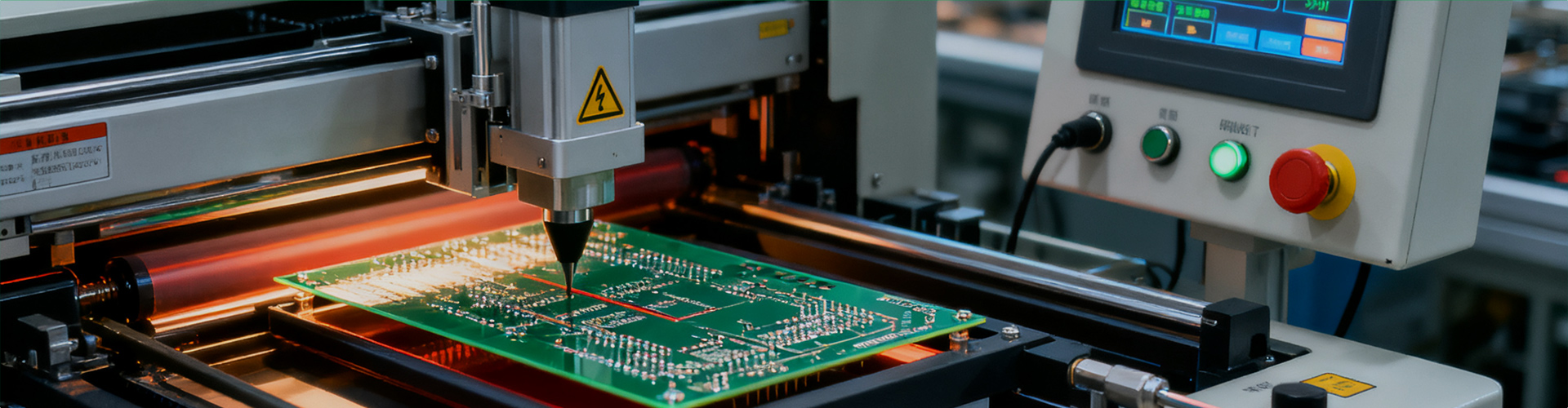
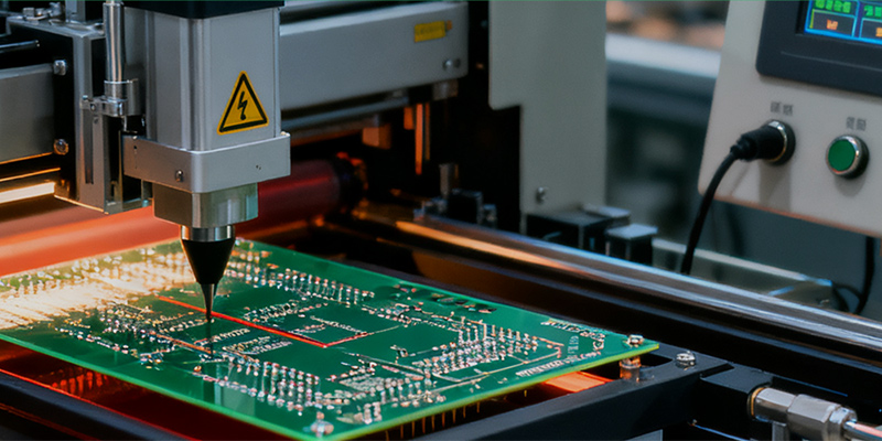
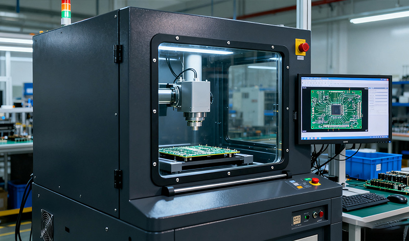
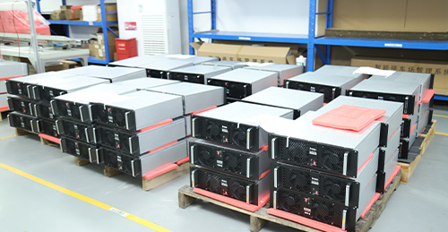
Prototype manufacturing is a critical link in the product design process, providing a reliable physical basis to ensure the feasibility of product design and prepare the product for trial production. It is also an essential step conducted before mass production to test product functions and verify that product performance and various indicators meet customer requirements, directly influencing the product's profitability after its market launch.
To reduce development costs, help customers accurately seize the product market window of opportunity, and accelerate product launch, our prototype manufacturing services adhere to the optimization principle of integrating design, production, and functional testing. Starting from the initial PCB (Printed Circuit Board) design phase, we incorporate functional simulation and testing concepts, minimizing the extended timeline and additional costs caused by rework in subsequent development and manufacturing processes to maximize benefits for our customers.
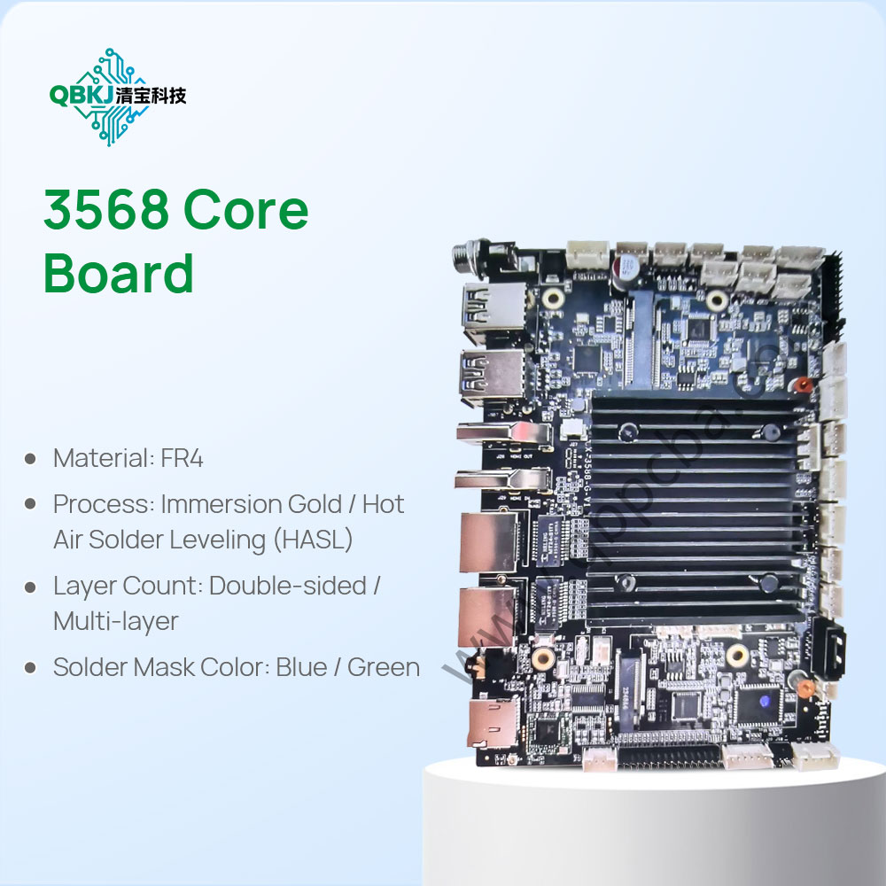
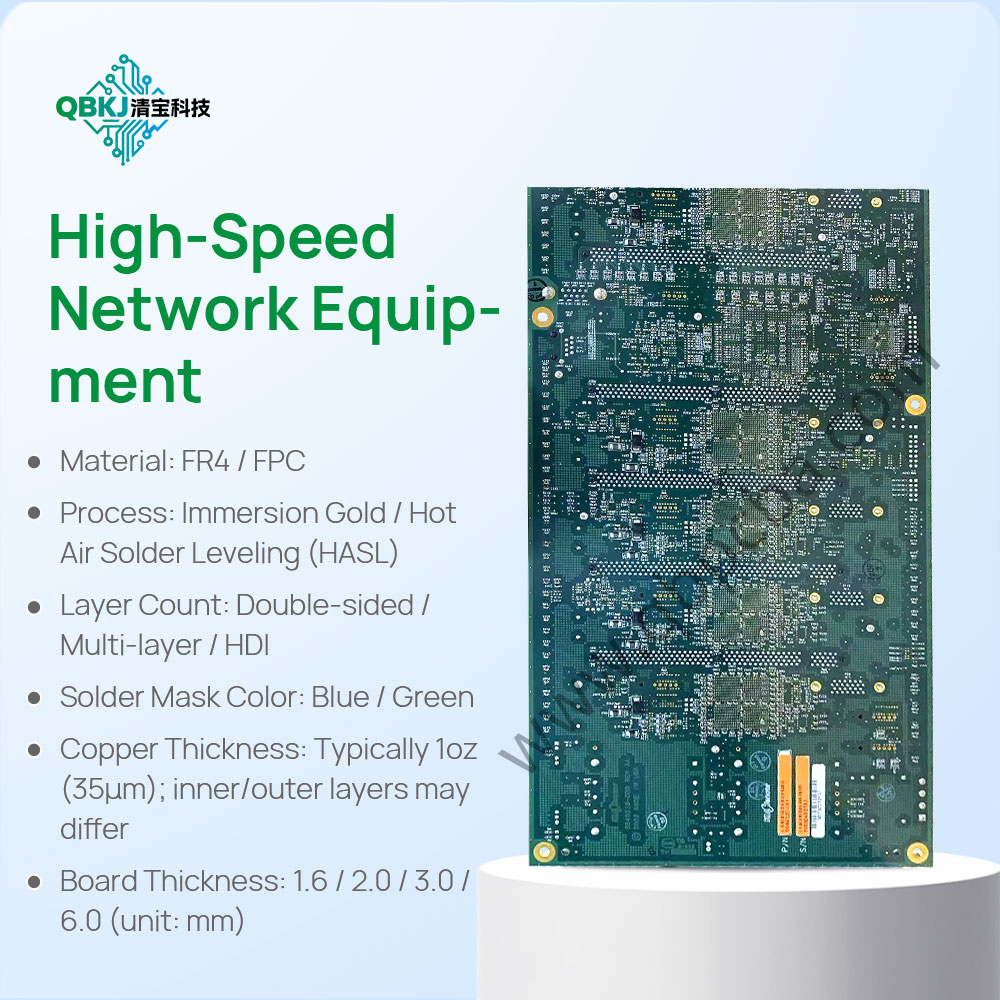
| Number of Layers | 1-20 Layers | ||
| HDI Structure | 1-2 Stages (for HDI PCBs) | Mechanical Blind/Buried Vias or Laser Blind/Buried Vias (Platable Hole Filling Available) | |
| Substrate Type | Shengyi: Tg140/Tg150/Tg180; Jiantao: Tg130/Tg150/Tg170 | ||
| Surface Finish | Lead/Lead-Free Hot Air Solder Leveling (HASL), lmmersion Gold, OSP | ||
| Board Thickness Range | 0.6-2.5mm | Standard Board Thickness: 0.6/0.8/1.0/1.2/1.6/2.0/2.5mm; For mass production, the maximum processable board thickness is 3.0mm | |
| Board Thickness Tolerance | T≥1.0mm±10% T<1.0mm±0.1mm | ||
| Laser Drill Hole Range | Applicable to blind via boards, tolerance for laser vias is ±0.01mm | ||
| Mechanical Drill Hole Range | 0.15-6.35mm | Minimum drill hole diameter: 0.15mm; maximum drill bit size: 6.35mm; holeslarger than 6.35mm require additional processing | |
| Minimum Metal Slot | 0.45mm | Tolerance for slotted hole diameter: ±0.1mm | |
| Minimum Non-Metal Slot | 0.8mm | Minimum routing bit size: 0.8mm | |
| Drill Hole Aspect Ratio | 10:1 | For a 0.2mm hole, the maximum processable board thickness is 2.0mm | |
Hole Position Tolerance | ≤0.075mm | ||
| Hole Diameter Tolerance | PTH NPTH | ±0.075mm ±0.05mm | Hole DiameterTolerance for Metalized Holes Hole Diameter Tolerance for Non-Metalized Holes |
| Minimum Inner-Layer Line Width/Space | 0.50z | 3/3mil | |
PCB Copying
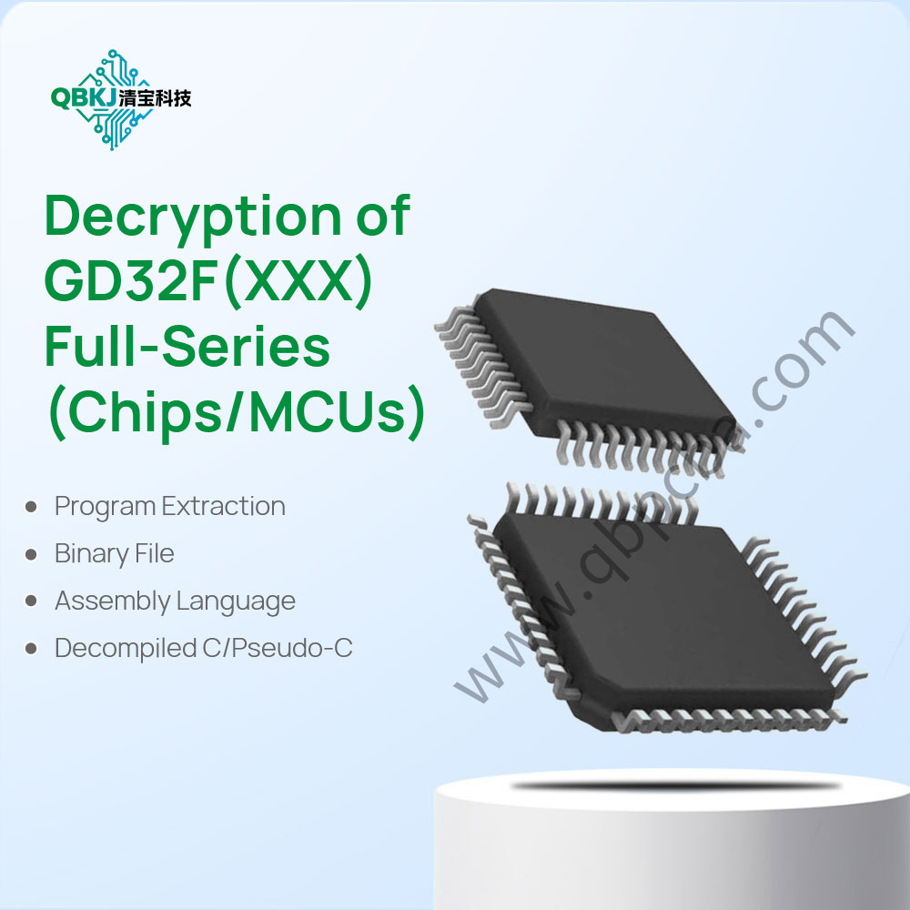
Chip Decryption
PCB Manufacturing
PCBA OEM
PCB Copying
Chip Decryption
PCB Manufacturing
PCBA OEM
PCB Copying
Chip Decryption
PCB Manufacturing
PCBA OEM
PCB Copying
Chip Decryption
PCB Manufacturing
PCBA OEM
PCB Copying
Chip Decryption
PCB Manufacturing
PCBA OEM
PCB Copying
Chip Decryption
PCB Manufacturing
PCBA OEM
PCB Copying
Chip Decryption
PCB Manufacturing
PCBA OEM
PCB Copying
Chip Decryption
PCB Manufacturing
PCBA OEM

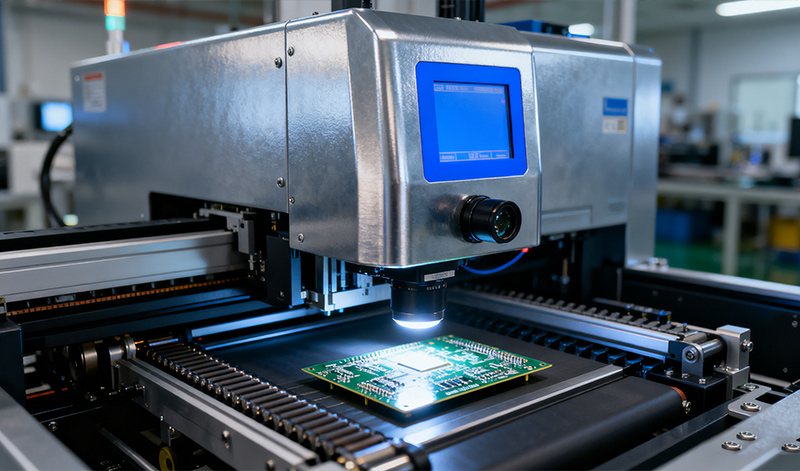
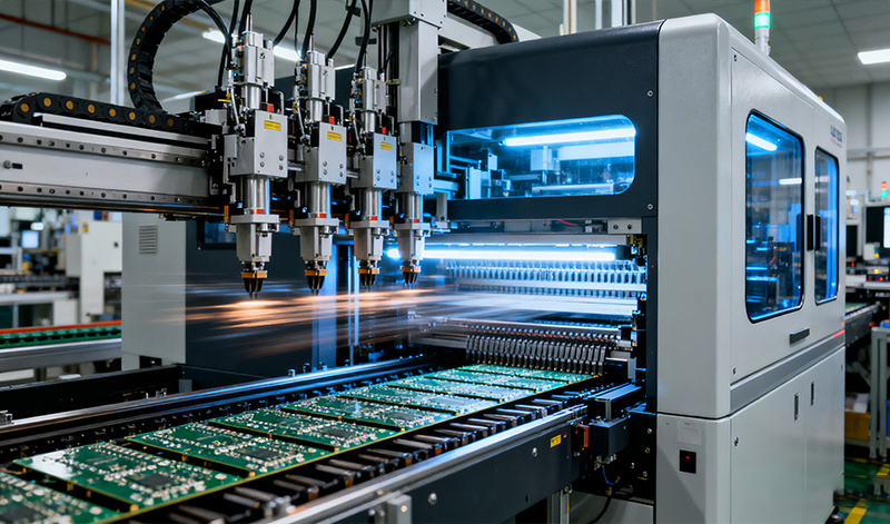
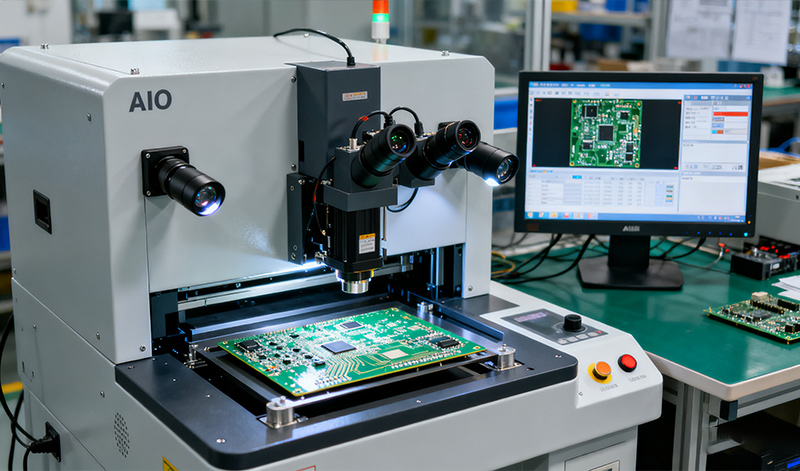
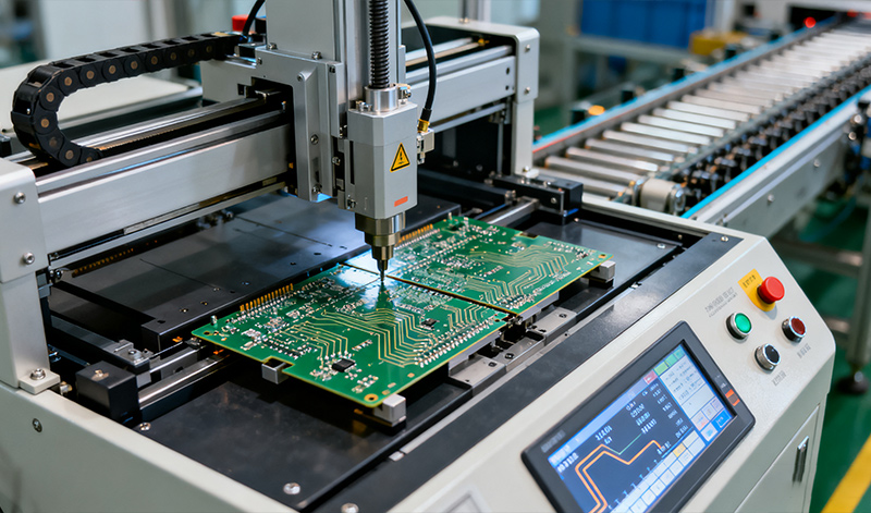
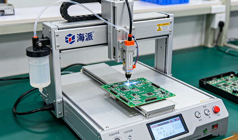
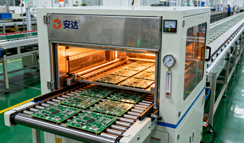
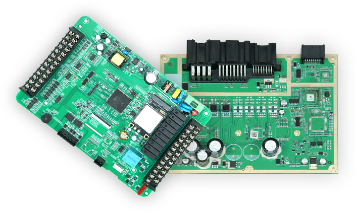
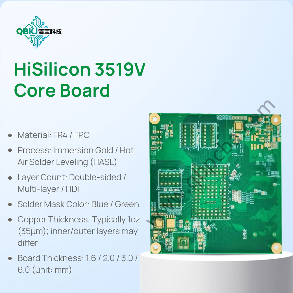
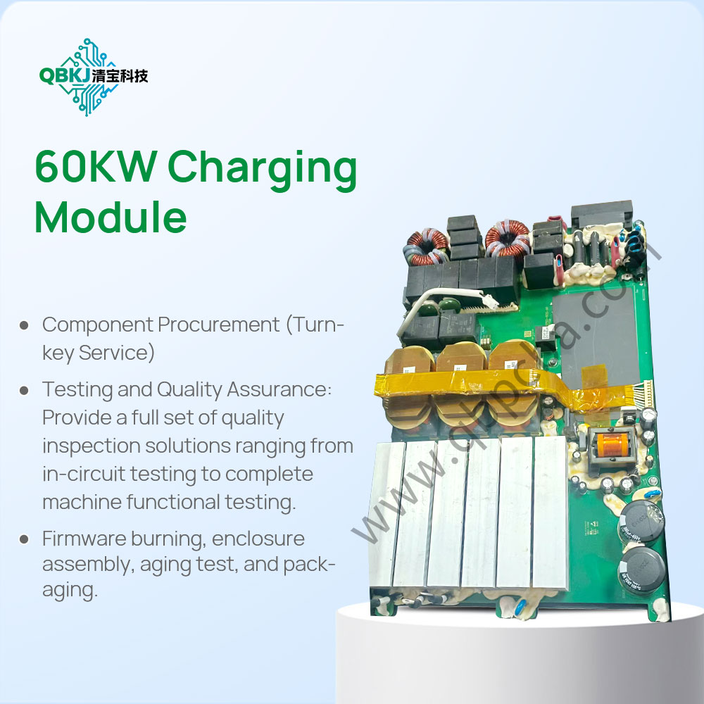
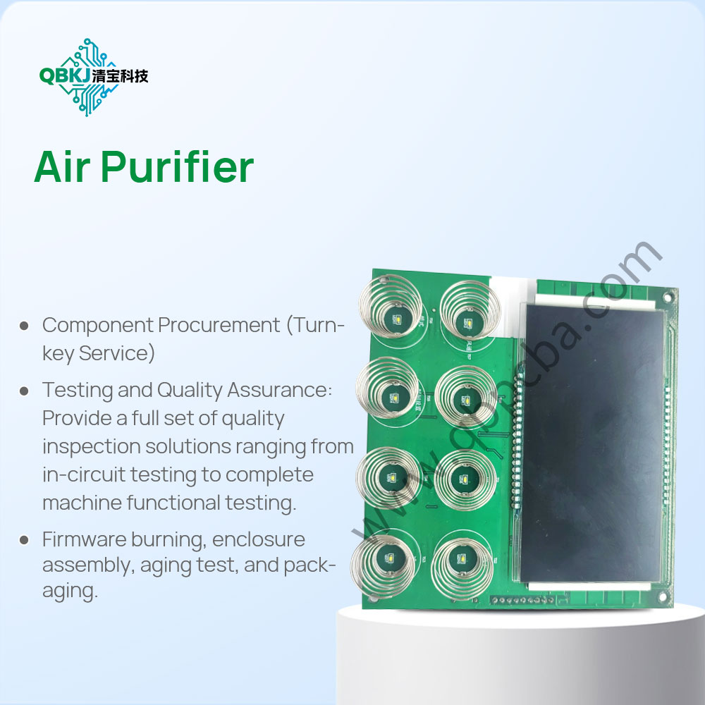
We provide cloning services for single-layer, double-layer, and multi-layer PCBs (up to 32 layers). We are capable of cloning high-difficulty PCBs such as various blind and buried via PCBs. Based on the intact prototype board or sample machine provided, we can achieve one-time cloning success and guarantee 100% consistency with the original PCB circuit.
We provide cloning services for single-layer, double-layer, and multi-layer PCBs (up to 32 layers). We are capable of cloning high-difficulty PCBs such as various blind and buried via PCBs. Based on the intact prototype board or sample machine provided, we can achieve one-time cloning success and guarantee 100% consistency with the original PCB circuit.
We provide cloning services for single-layer, double-layer, and multi-layer PCBs (up to 32 layers). We are capable of cloning high-difficulty PCBs such as various blind and buried via PCBs. Based on the intact prototype board or sample machine provided, we can achieve one-time cloning success and guarantee 100% consistency with the original PCB circuit.
We provide cloning services for single-layer, double-layer, and multi-layer PCBs (up to 32 layers). We are capable of cloning high-difficulty PCBs such as various blind and buried via PCBs. Based on the intact prototype board or sample machine provided, we can achieve one-time cloning success and guarantee 100% consistency with the original PCB circuit.
Provide Diversified Customization Services
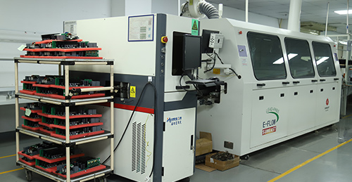
6-Axis High-Speed Drilling Machine
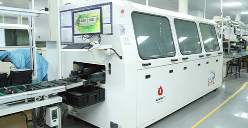
Automatic PTH Copper Deposition and Desmear Integrated Line
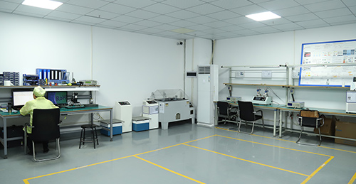
High-Reliability Physical Laboratory and Chemical Laboratory
Email: 1330695973@qq.com
Factory: Room 703, Kelunte R&D Building, No. 1 Ganli 5th Road, Jihua Street, Longgang District, Shenzhen City